Connectors#
This section describes each of the connectors on the board.
Expansion Header Connectors#
The expansion interface on the board is comprised of two 36 pin connectors. The two Expansion Header Connectors on PocketBeagle are labeled P1 and P2. The connections are a standard 100 mil distance so that they can be compatible with many standard expansion items. The silkscreen for the headers on the bottom of the board provides the easiest way to identify them. See Figure 41.
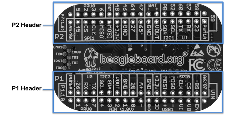
Fig. 301 Expansion Headers for PocketBeagle#
All signals on the expansion headers are 3.3V unless otherwise indicated.
Note
Do not connect 5V logic level signals to these pins or the board will be damaged.
DO NOT APPLY VOLTAGE TO ANY I/O PIN WHEN POWER IS NOT SUPPLIED TO THE BOARD. IT WILL DAMAGE THE PROCESSOR AND VOID THE WARRANTY.
NO PINS ARE TO BE DRIVEN UNTIL AFTER THE NRESET LINE GOES HIGH.
Figure 42 shows a color coded chart with an overview of the most popular functions of PocketBeagle’s Expansion Header pins. The Header Pin tables in Sections 7.1.1 and 7.1.2 show the full pin assignments for each header.
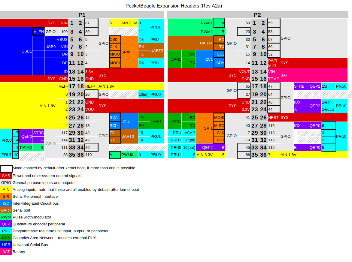
Fig. 302 Expansion Header Popular Functions - Color Coded#
P1 Header#
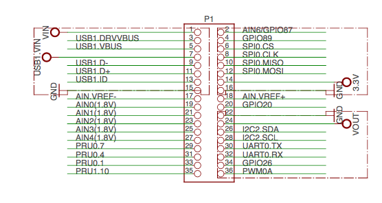
Figure 43 shows the schematic diagram for the P1 Header.
Use scroll bar at bottom of chart to see additional features in columns to the right. When printing this document you will need to print this chart separately.
Header.Pin |
Silkscreen |
PocketBeagle wiring |
Proc Ball |
SiP Ball |
Mode0 (Name) |
Mode1 |
Mode2 |
Mode3 |
Mode4 |
Mode5 |
Mode6 |
Mode7 |
|---|---|---|---|---|---|---|---|---|---|---|---|---|
P1.01 |
VIN |
P1.01 (VIN) |
P10 & R10 & T10 |
VIN |
||||||||
P1.02 |
A6/87 |
P1.02 (AIN6/GPIO87) |
A8 |
C9 |
ain6 |
|||||||
P1.02 |
A6/87 |
P1.02 (AIN6/GPIO87) |
R5 |
F2 |
lcd_hsync |
gpmc_a9 |
gpmc_a2 |
pr1_edio_data_in3 |
pr1_edio_data_out3 |
pr1_pru1_pru_r30_9 |
pr1_pru1_pru_r31_9 |
gpio2_23 |
P1.03 |
USB1_EN |
P1.03 (USB1-DRVVBUS) |
F15 |
M14 |
USB1_DRVVBUS |
gpio3_13 |
||||||
P1.04 |
89 |
P1.04 (PRU1.11) |
R6 |
E1 |
lcd_ac_bias_en |
gpmc_a11 |
pr1_mii1_crs |
pr1_edio_data_in5 |
pr1_edio_data_out5 |
pr1_pru1_pru_r30_11 |
pr1_pru1_pru_r31_11 |
gpio2_25 |
P1.05 |
USB1_VB |
P1.05 (USB1-VBUS) |
T18 |
M15 |
USB1_VBUS |
|||||||
P1.06 |
SPI0_CS |
P1.06 (SPI0-CS) |
A16 |
A14 |
spi0_cs0 |
mmc2_sdwp |
I2C1_SCL |
ehrpwm0_synci |
pr1_uart0_txd |
pr1_edio_data_in1 |
pr1_edio_data_out1 |
gpio0_5 |
P1.07 |
USB1_VI |
P1.07 (VIN-USB) |
P9 &R9 &T9 |
VIN-USB |
||||||||
P1.08 |
SPI0_CLK |
P1.08 (SPI0-CLK) |
A17 |
A13 |
spi0_sclk |
uart2_rxd |
I2C2_SDA |
ehrpwm0A |
pr1_uart0_cts_n |
pr1_edio_sof |
EMU2 |
gpio0_02 |
P1.09 |
USB1 - |
P1.09 (USB1-DN) |
R18 |
L16 |
USB1_DM |
|||||||
P1.10 |
SPI0_MISO |
P1.10 (SPI0-MISO) |
B17 |
B13 |
spi0_d0 |
uart2_txd |
I2C2_SCL |
ehrpwm0B |
pr1_uart0_rts_n |
pr1_edio_latch_in |
EMU3 |
gpio0_3 |
P1.11 |
USB1 + |
P1.11 (USB1-DP) |
R17 |
L15 |
USB1_DP |
|||||||
P1.12 |
SPI0_MOSI |
P1.12 (SPI0-MOSI) |
B16 |
B14 |
spi0_d1 |
mmc1_sdwp |
I2C1_SDA |
ehrpwm0_tripzone_input |
pr1_uart0_rxd |
pr1_edio_data_in0 |
pr1_edio_data_out0 |
gpio0_04 |
P1.13 |
USB1_ID |
P1.13 (USB1-ID) |
P17 |
L14 |
USB1_ID |
|||||||
P1.14 |
+3.3V |
P1.14 (VOUT-3.3V) |
F6 & F7 & G6 & G7 |
VOUT-3.3V |
||||||||
P1.15 |
USB1_GND |
P1.15 (GND) |
GND |
|||||||||
P1.16 |
GND |
P1.16 (GND) |
GND |
|||||||||
P1.17 |
AIN(1.8V)- |
P1.17 (VREFN) |
A9 |
B9 |
VREFN |
|||||||
P1.18 |
AIN(1.8V)A+ |
P1.18 (VREFP) |
B9 |
B7 |
VREFP |
|||||||
P1.19 |
AIN(1.8V)0 |
P1.19 (AIN0-1.8V) |
B6 |
A8 |
ain0 |
|||||||
P1.20 |
20 |
P1.20 (PRU0.16) |
D14 |
B4 |
xdma_event_intr1 |
tclkin |
clkout2 |
timer7 |
pr1_pru0_pru_r31_16 |
EMU3 |
gpio0_20 |
|
P1.21 |
AIN(1.8V)1 |
P1.21 (AIN1-1.8V) |
C7 |
B8 |
ain1 |
|||||||
P1.22 |
GND |
P1.22 (GND) |
GND |
|||||||||
P1.23 |
AIN(1.8V)2 |
P1.23 (AIN2-1.8V) |
B7 |
B6 |
ain2 |
|||||||
P1.24 |
VOUT |
P1.24 (VOUT-5V) |
K6 & K7 & L6 & L7 |
VOUT-5V |
||||||||
P1.25 |
AIN(1.8V)3 |
P1.25 (AIN3-1.8V) |
A7 |
C6 |
ain3 |
|||||||
P1.26 |
I2C2_SDA |
P1.26 (I2C2-SDA) |
D18 |
B10 |
uart1_ctsn |
timer6 |
dcan0_tx |
I2C2_SDA |
spi1_cs0 |
pr1_uart0_cts_n |
pr1_edc_latch0_in |
gpio0_12 |
P1.27 |
AIN(1.8V)4 |
P1.27 (AIN4-1.8V) |
C8 |
C7 |
ain4 |
|||||||
P1.28 |
I2C2_SCL |
P1.28 (I2C2-SCL) |
D17 |
A10 |
uart1_rtsn |
timer5 |
dcan0_rx |
I2C2_SCL |
spi1_cs1 |
pr1_uart0_rts_n |
pr1_edc_latch1_in |
gpio0_13 |
P1.29 |
PRU0_7 |
P1.29 (PRU0.7) |
A14 |
C4 |
mcasp0_ahclkx |
eQEP0_strobe |
mcasp0_axr3 |
mcasp1_axr1 |
EMU4 |
pr1_pru0_pru_r30_7 |
pr1_pru0_pru_r31_7 |
gpio3_21 |
P1.30 |
U0_TX |
P1.30 (UART0-TX) |
E16 |
B12 |
uart0_txd |
spi1_cs1 |
dcan0_rx |
I2C2_SCL |
eCAP1_in_PWM1_out |
pr1_pru1_pru_r30_15 |
pr1_pru1_pru_r31_15 |
gpio1_11 |
P1.31 |
PRU0_4 |
P1.31 (PRU0.4) |
B12 |
A3 |
mcasp0_aclkr |
eQEP0A_in |
mcasp0_axr2 |
mcasp1_aclkx |
mmc0_sdwp |
pr1_pru0_pru_r30_4 |
pr1_pru0_pru_r31_4 |
gpio3_18 |
P1.32 |
U0_RX |
P1.32 (UART0-RX) |
E15 |
A12 |
uart0_rxd |
spi1_cs0 |
dcan0_tx |
I2C2_SDA |
eCAP2_in_PWM2_out |
pr1_pru1_pru_r30_14 |
pr1_pru1_pru_r31_14 |
gpio1_10 |
P1.33 |
PRU0_1 |
P1.33 (PRU0.1) |
B13 |
A2 |
mcasp0_fsx |
ehrpwm0B |
spi1_d0 |
mmc1_sdcd |
pr1_pru0_pru_r30_1 |
pr1_pru0_pru_r31_1 |
gpio3_15 |
|
P1.34 |
26 |
P1.34 (GPIO0.26) |
T11 |
R5 |
gpmc_ad10 |
lcd_data21 |
mmc1_dat2 |
mmc2_dat6 |
ehrpwm2_tripzone_input |
pr1_mii0_txen |
gpio0_26 |
|
P1.35 |
P1.10 |
P1.35 (PRU1.10) |
V5 |
F1 |
lcd_pclk |
gpmc_a10 |
pru_mii0_crs |
pr1_edio_data_in4 |
pr1_edio_data_out4 |
pr1_pru1_pru_r30_10 |
pr1_pru1_pru_r31_10 |
gpio2_24 |
P1.36 |
PWM0A |
P1.36 (PWM0A) |
A13 |
A1 |
mcasp0_aclkx |
ehrpwm0A |
spi1_sclk |
mmc0_sdcd |
pr1_pru0_pru_r30_0 |
pr1_pru0_pru_r31_0 |
gpio3_14 |
P2 Header#
Figure 44 shows the schematic diagram for the P2 Header.
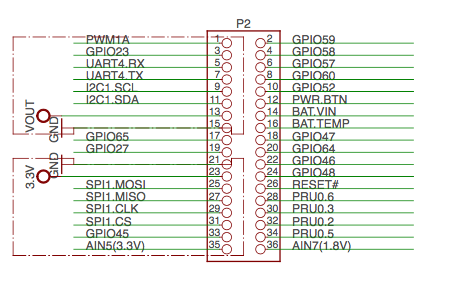
Fig. 303 P2 Header#
Use scroll bar at bottom of chart to see additional features in columns to the right. When printing this document you will need to print this chart separately.
Header.Pin |
Silkscreen |
PocketBeagle wiring |
Proc Ball |
SiP Ball |
Mode0 (Name) |
Mode1 |
Mode2 |
Mode3 |
Mode4 |
Mode5 |
Mode6 |
Mode7 |
|---|---|---|---|---|---|---|---|---|---|---|---|---|
P2.01 |
PWM1A |
P2.01 (PWM1A) |
U14 |
P12 |
gpmc_a2 |
gmii2_txd3 |
rgmii2_td3 |
mmc2_dat1 |
gpmc_a18 |
pr1_mii1_txd2 |
ehrpwm1A |
gpio1_18 |
P2.02 |
59 |
P2.02 (GPIO1.27) |
V17 |
T16 |
gpmc_a11 |
gmii2_rxd0 |
rgmii2_rd0 |
rmii2_rxd0 |
gpmc_a27 |
pr1_mii1_rxer |
mcasp0_axr1 |
gpio1_27 |
P2.03 |
23 |
P2.03 (GPIO0.23) |
T10 |
P5 |
gpmc_d9 |
lcd_data22 |
mmc1_dat1 |
mmc2_dat5 |
ehrpwm2B |
pr1_mii0_col |
gpio0_23 |
|
P2.04 |
58 |
P2.04 (GPIO1.26) |
T16 |
R15 |
gpmc_a10 |
gmii2_rxd1 |
rgmii2_rd1 |
rmii2_rxd1 |
gpmc_a26 |
pr1_mii1_rxdv |
mcasp0_axr0 |
gpio1_26 |
P2.05 |
U1_RX |
P2.05 (UART4-RX) |
T17 |
P15 |
gpmc_wait0 |
gmii2_crs |
gpmc_csn4 |
rmii2_crs_dv |
mmc1_sdcd |
pr1_mii1_col |
uart4_rxd |
gpio0_30 |
P2.06 |
57 |
P2.06 (GPIO1.25) |
U16 |
T15 |
gpmc_a9 |
gmii2_rxd2 |
rgmii2_rd2 |
mmc2_dat7 / rmii2_crs_dv |
gpmc_a25 |
pr1_mii_mr1_clk |
mcasp0_fsx |
gpio1_25 |
P2.07 |
U1_TX |
P2.07 (UART4-TX) |
U17 |
R16 |
gpmc_wp |
gmii2_rxerr |
gpmc_csn5 |
rmii2_rxerr |
mmc2_sdcd |
pr1_mii1_txen |
uart4_txd |
gpio0_31 |
P2.08 |
60 |
P2.08 (GPIO1.28) |
U18 |
N14 |
gpmc_be1n |
gmii2_col |
gpmc_csn6 |
mmc2_dat3 |
gpmc_dir |
pr1_mii1_rxlink |
mcasp0_aclkr |
gpio1_28 |
P2.09 |
I2C1_SCL |
P2.09 (I2C1-SCL) |
D15 |
B11 |
uart1_txd |
mmc2_sdwp |
dcan1_rx |
I2C1_SCL |
pr1_uart0_txd |
pr1_pru0_pru_r31_16 |
gpio0_15 |
|
P2.10 |
52 |
P2.10 (GPIO1.20) |
R14 |
R13 |
gpmc_a4 |
gmii2_txd1 |
rgmii2_td1 |
rmii2_txd1 |
gpmc_a20 |
pr1_mii1_txd0 |
eQEP1A_in |
gpio1_20 |
P2.11 |
I2C1_SDA |
P2.11 (I2C1-SDA) |
D16 |
A11 |
uart1_rxd |
mmc1_sdwp |
dcan1_tx |
I2C1_SDA |
pr1_uart0_rxd |
pr1_pru1_pru_r31_16 |
gpio0_14 |
|
P2.12 |
PB |
P2.12 (POWER_BTN) |
T11 |
POWER |
||||||||
P2.13 |
VOUT |
P2.13 (VOUT-5V) |
K6, K7, L6, L7 |
VOUT-5V |
||||||||
P2.14 |
BAT + |
P2.14 (VIN-BAT) |
P8, R8, T8 |
VIN-BAT |
||||||||
P2.15 |
GND |
P2.15 (GND) |
GND |
|||||||||
P2.16 |
BAT - |
P2.16 (BAT-TEMP) |
N6 |
BAT-TEMP |
||||||||
P2.17 |
65 |
P2.17 (GPIO2.1) |
V12 |
T7 |
gpmc_clk |
lcd_memory_clk |
gpmc_wait1 |
mmc2_clk |
pr1_mii1_crs |
pr1_mdio_mdclk |
mcasp0_fsr |
gpio2_01 |
P2.18 |
47 |
P2.18 (PRU0.15i) |
U13 |
P7 |
gpmc_ad15 |
lcd_data16 |
mmc1_dat7 |
mmc2_dat3 |
eQEP2_strobe |
pr1_ecap0_ecap_capin_apwm_o |
pr1_pru0_pru_r31_15 |
gpio1_15P |
P2.19 |
27 |
P2.19 (GPIO0.27) |
U12 |
T5 |
gpmc_ad11 |
lcd_data20 |
mmc1_dat3 |
mmc2_dat7 |
ehrpwm0_synco |
pr1_mii0_txd3 |
gpio0_27 |
|
P2.20 |
64 |
P2.20 (GPIO2.0) |
T13 |
R7 |
gpmc_csn3 |
gpmc_a3 |
rmii2_crs_dv |
mmc2_cmd |
pr1_mii0_crs |
pr1_mdio_data |
EMU4 |
gpio2_00 |
P2.21 |
GND |
P2.21 (GND) |
GND |
|||||||||
P2.22 |
46 |
P2.22 (GPIO1.14) |
V13 |
T6 |
gpmc_ad14 |
lcd_data17 |
mmc1_dat6 |
mmc2_dat2 |
eQEP2_index |
pr1_mii0_txd0 |
pr1_pru0_pru_r31_14 |
gpio1_14 |
P2.23 |
+3.3V |
P2.23 (VOUT-3.3V) |
F6 & F7 & G6 & G7 |
VOUT-3.3V |
||||||||
P2.24 |
48 |
P2.24 (GPIO1.12) |
T12 |
P6 |
gpmc_ad12 |
lcd_data19 |
mmc1_dat4 |
mmc2_dat0 |
eQEP2A_in |
pr1_mii0_txd2 |
pr1_pru0_pru_r30_14 |
gpio1_12 |
P2.25 |
SPI1_MOSI |
P2.25 (SPI1-MOSI) |
E17 |
C13 |
uart0_rtsn |
uart4_txd |
dcan1_rx |
I2C1_SCL |
spi1_d1 |
spi1_cs0 |
pr1_edc_sync1_out |
gpio1_09 |
P2.26 |
RST |
P2.26 (NRESET) |
A10 |
R11 |
nRESETIN_OUT |
|||||||
P2.27 |
SPI1_MISO |
P2.27 (SPI1-MISO) |
E18 |
C12 |
uart0_ctsn |
uart4_rxd |
dcan1_tx |
I2C1_SDA |
spi1_d0 |
timer7 |
pr1_edc_sync0_out |
gpio1_08 |
P2.28 |
PRU0_6 |
P2.28 (PRU0.6) |
D13 |
C3 |
mcasp0_axr1 |
eQEP0_index |
mcasp1_axr0 |
EMU3 |
pr1_pru0_pru_r30_6 |
pr1_pru0_pru_r31_6 |
gpio3_20 |
|
P2.29 |
SPI1_CLK |
P2.29 (SPI1-CLK) |
C18 |
C5 |
eCAP0_in_PWM0_out |
uart3_txd |
spi1_cs1 |
pr1_ecap0_ecap_capin_apwm_o |
spi1_sclk |
mmc0_sdwp |
xdma_event_intr2 |
gpio0_7 |
P2.30 |
PRU0_3 |
P2.30 (PRU0.3) |
C12 |
B1 |
mcasp0_ahclkr |
ehrpwm0_synci |
mcasp0_axr2 |
spi1_cs0 |
eCAP2_in_PWM2_out |
pr1_pru0_pru_r30_3 |
pr1_pru0_pru_r31_3 |
gpio3_17 |
P2.31 |
SPI1_CS |
P2.31 (SPI1-CS1) |
A15 |
A4 |
xdma_event_intr0 |
timer4 |
clkout1 |
spi1_cs1 |
pr1_pru1_pru_r31_16 |
EMU2 |
gpio0_19 |
|
P2.32 |
PRU0_2 |
P2.32 (PRU0.2) |
D12 |
B2 |
mcasp0_axr0 |
ehrpwm0_tripzone_input |
spi1_d1 |
mmc2_sdcd |
pr1_pru0_pru_r30_2 |
pr1_pru0_pru_r31_2 |
gpio3_16 |
|
P2.33 |
45 |
P2.33 (GPIO1.13) |
R12 |
R6 |
gpmc_ad13 |
lcd_data18 |
mmc1_dat5 |
mmc2_dat1 |
eQEP2B_in |
pr1_mii0_txd1 |
pr1_pru0_pru_r30_15 |
gpio1_13 |
P2.34 |
PRU0_5 |
P2.34 (PRU0.5) |
C13 |
B3 |
mcasp0_fsr |
eQEP0B_in |
mcasp0_axr3 |
mcasp1_fsx |
EMU2 |
pr1_pru0_pru_r30_5 |
pr1_pru0_pru_r31_5 |
gpio3_19 |
P2.35 |
A5/86 |
P2.35 (AIN5/GPIO86) |
B8 |
C8 |
ain5 |
|||||||
P2.35 |
A5/86 |
P2.35 (AIN5/GPIO86) |
U5 |
F3 |
lcd_vsync |
gpmc_a8 |
gpmc_a1 |
pr1_edio_data_in2 |
pr1_edio_data_out2 |
pr1_pru1_pru_r30_8 |
pr1_pru1_pru_r31_8 |
gpio2_22 |
P2.36 |
A7(1.8) |
P2.36 (AIN7) |
N13 |
ain7 |
mikroBUS socket connections#
mikroBUS and, by extension “mikroBUS Click boards”, are trademarks of MikroElektronika. We do not make any claims of compatibility nor adherence to their specification. We’ve just seen that many of the Click boards “just work”.
The Expansion Headers on PocketBeagle have been designed to accept up to two Click Boards added to the header pins at the same time. This provides an exciting opportunity to add functionality easily to PocketBeagle from ‘hundreds of existing add-on Click Boards’.
The mikroBUS standard comprises a pair of 1×8 female headers with a standardized pin configuration. The pinout (always laid out in the same order) consists of three groups of communications pins (SPI, UART and I2C), six additional pins (PWM, Interrupt, Analog input, Reset and Chip select), and two power groups (+3.3V and 5V).
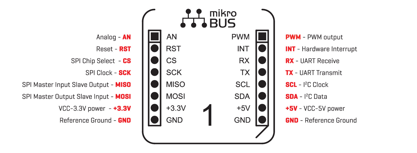
Fig. 304 mikroBUS#
The Expansion Header pin alignment enables 2 Click Boards on the top side of PocketBeagle using the inside rails of the headers. This leaves the outside rails open to be accessed from either the top or the bottom of PocketBeagle. Place each Click Board into the position shown in Figure 46, with one Click Board facing each direction. When choosing Click boards, make sure you are checking that they meet the 3.3V requirements for PocketBeagle. A growing number of community members are trying out various Click Boards and posting results on the ‘PocketBeagle Wiki mikroBus Click Boards page’.

Fig. 305 PocketBeagle Both Headers#
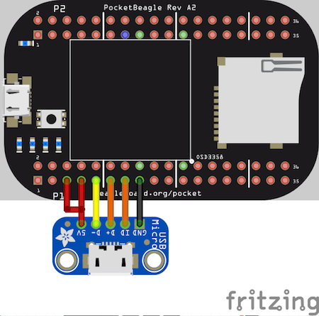
Setting up an additional USB Connection#
You can add an additional USB connection to PocketBeagle easily by connecting a microUSB breakout. By default in the current software, the system should be configured to use this port as a host. Keep up to date on this project on the ‘PocketBeagle Wiki FAQ’.
